How To Shine
With the LED boards up and running, it’s now time to look into firmware that will make them shine.
Listen Up!
Inspiration
The de facto standard to control a bunch of lamps on a data bus is DMX512. As this project has that same form, using the DMX512 protocol would seem obvious. However, it transpired that a clean DMX512 implementation wasn’t going to work for this design. So in the end I spun my own version of a protocol, inspired by DMX512. For a proper explanation visit the protocol’s Wikipedia page. To understand how it inspired my Party Lights Protocol, read on.
Very simply put, DMX512 is just a series of bytes representing the light intensities of a series of lamps, preceded by a synchronization signal. The first byte represents a start code. The succeeding bytes each represent one of the nodes on the bus. The position of the byte in the stream corresponds to the address of the node (addresses being set at each receiving node). The synchronization signal consists of a Break symbol (the bus going low for 100us) followed by a Mark After Break (MAB) symbol (the bus being high for 12us).
Being In Sync
So, Why not just adopt the DMX512 protocol? Because of the synchronization wasn’t going to work. The LED nodes have very low end microcontrollers that run their clocks from an internal RC-oscillator. The light controller is not as low end, but also runs from an RC-oscillator. For both designs this was done so as a cost saving measure. As a consequence, the clocks are wildly inaccurate and and not even near the timing specification for the Attiny UART peripheral. DMX512 has a synchronization pulse, but just one. I wasn’t confident that the receiving nodes would be able to sample that pulse accurately enough to synchronize to.
The Party Lights Protocol (let’s just name it that way because it’s so cool to have our own protocol) tackles the synchronization issue by adding a burst signal at the beginning of each transmission. The transmission starts with a blanking period to indicate the beginning of the data transfer. Then follows the burst signal that consists of eight edges (alternatively rising and falling). The Attiny measures the time between these transitions by resetting Timer/Counter B at each edge of the burst signal.
In order to configure the UART baud rate, the BAUD register must be set. The value for that register can be derived from the CPU frequency and the desired baud rate. The formula is given by the datasheet and boils down to:
$$ BAUD = \dfrac{4 * f_{cpu}}{f_{baud}} $$With the desired baud rate being 250 kBaud and the CPU running at 20MHz, the BAUD register must be set to 320.
The time between the burst pulses is 32us. Timer/Counter B runs at the same frequency as the CPU (no prescaler). One CPU clock cycle takes 50ns, so in the 32us to the next edge, it counts to 640. The counter values are added up over the eight burst transitions and are then divided by 16. The result happens to be just the value the BAUD register needs for the desired baud rate: 320,
If the controller board runs at a CPU frequency that is higher than nominal, the pulses from the burst signal will be shorter. A higher baud rate will demand a lower value for the Baud Rate register of the Attiny. And that’s exactly what it gets!
In an ideal world, the Timer/Counter value exactly matches the pulse timing. In reality however, there are some inaccuracies because it takes some time for the microcontroller to jump to the interrupt service routine that starts the timer. I addressed this by making the pulse time relatively long so that the percentage error in timing gets smaller. There is also a fixed correction embedded in the firmware, but that’s based on a rough estimation of how long the controller will take to handle an interrupt.
The Rules Of the Game
Just like with DMX512, the data follows after synchronization and each word represents the brightness of an LED. I say word, instead of byte, because the protocol works with 9 data bits, rather than 8. More on that below. As each node consists of four LEDs (Red, Green, Blue and White), the datagram for each node comprises of four 9-bit words. The first block of 4 words is designated for node 0, the second block for node 1, etc. Basically the same way DMX512 works, but with 9 bits (and a single stop bit instead of two) and without the start code.
A frame (a datagram addressing all nodes on the network) looks like this:
- A synchronization period of 80 us
- A burst signal, with 8 equally spaced edges.
- Red, Green, Blue, White intensity for each node, sequentially transmitted
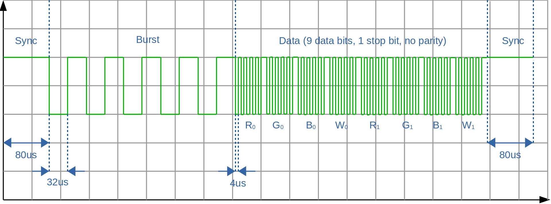 Communication protocol
Like with DMX512, there is no error detection (e.g. parity check). The frames are sent continuously and in quick succession. This means that any glitches in the data will just go unnoticed by the observer. A high frame rate is desirable for a smooth, glitch free light show, but not mandatory where the protocol is concerned. The maximum time allowed between frames is approximately one second. After this period the receiver enters sleep mode and turns off the LEDs.
The choice of 9 instead of 8 data bits has to do with maintaining sufficient resolution while dimming. An RGB color without dimming has 511 discrete steps for each color component. If we dim the light however, the color resolution drops, too. If the lights are dimmed to 10%, there are only 51 discrete steps left. This may not seem like a big deal, but if the colors change in time, there will come a point when the colors stop fading into each other smoothly, but appear as discrete steps instead. This isn’t pleasant to the eye and an extra bit resolution postpones the point at which it becomes annoying.
Message Received!
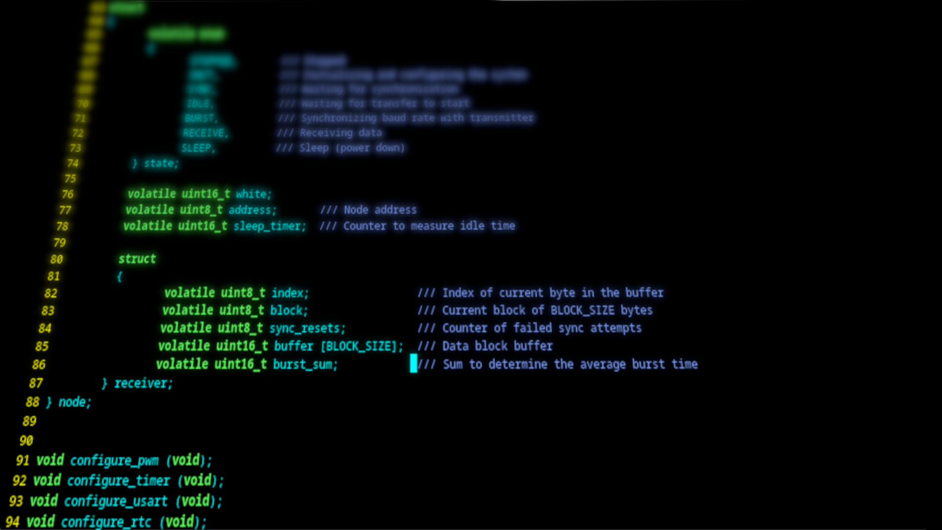
With the protocol in place, we can proceed to the implementation. The Attiny will be running a very simple C-program. Just C as there’s really no need for object oriented programming for a program this simple. The firmware is based around a single state machine.
The State of Affairs
The state diagram below outlines the states the LED node can be in and their transitions.
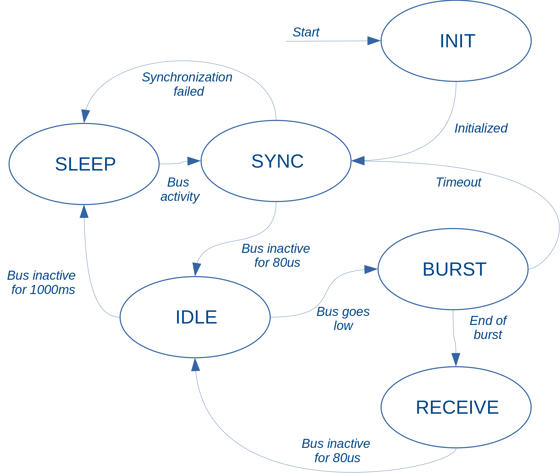 Receiver state diagram
Init state
After power-up the receiver enters the init state. Here the microcontroller peripherals are configured: the ports, the timers, PWM generation, UART, RTC and watchdog timer. The node address is also copied to RAM from the EEPROM. When the initialization is done the system enters the Sync state.
Sync State
In the Sync state the node waits until the bus remains in a high state for a predetermined time period of 80us. If the bus is low, the receiver waits for the bus to become high first. If that takes too long it is assumed something’s wrong and the receiver enters the Sleep state. Every time a falling edge is detected on the bus, the timer is reset and the synchronization attempt restarts. When the bus is high for long enough, the Timer/Counter times out and the synchronization ends. The system then enters the Idle state.
Idle State
In this state the receiver patiently waits for the burst signal to come. If it doesn’t, it enters the Sleep state after approximately one second. If during the Idle state a pin change interrupt occurs, the receiver enters the Burst state.
Burst State
The Burst state makes sure the right Baud rate is set before the data is being received. Upon entering this state, a Timer/Counter is started. At each detected edge the Timer/Counter is sampled and then reset. After eight successive edges the average timer value is calculated. The average value is then divided to form an appropriate value for the USART0.BAUD register. At this point the receiver enters the Receive state. If the burst signal is invalid, the system returns to the Sync state.
Receive State
Unsurprisingly, in this state the data will be received. The UART peripheral is enabled and an interrupt is generated whenever a byte has been received. A block counter is increased by one after every fourth word. If the block counter matches the address of the node, then the data is copied to the PWM registers for the Red, Green and Blue lights. The data for the white channel is converted to a bit sequence that represents the appropriate duty cycle for the white LED. The Receive state ends when no data has been received for 80us. The receiver then returns to the Idle state.
Sleep State
The Sleep state is a power saving mode that is engaged when no data has been received for about one second. The LEDs are turned off and the UART and watchdog timer are disabled. The pin change interrupt is enabled so any bus activity will trigger the receiver to continue work. The microcontroller does not enter low power mode. I’ll explain why in a bit.
Who Am I, Anyway?
How do the LED nodes know to which data block they are to respond? Well, they remember who they are. They remember their address, that is. The address is stored in EEPROM.
The original plan was to add a factory mode with which the address would be programmed using the test jig. But as I had already run out of flash space with just the basic functionality, this couldn’t be implemented. As an alternative the UPDI programming port must now be used to set the address.
Incidentally, if anyone has experience in writing the EEPROM from firmware in an AVR0, please tell me how it’s done! I found the datasheet (as well as any related application notes) utterly incomprehensible regarding the matter.
Talking Pulse With Modulation
In the blog post on the hardware design for the lamp nodes I already discussed the hack that makes the PWM for the white LEDs work. The UART transmitter is being used for that.
What will be effective PWM frequency? Well, a single UART frame with 9 data bits and a single start and stop bit consists of 11 bits. At 250 kBaud, the bit time is 4us. A single frame (or a single pulse, if you will) takes 44us, which comes down to 22.2 kHz.
With this UART hack the PWM resolution is limited, but it could potentially be improved somewhat by using not one, but two 9 bit words to generate the signal. Unfortunately, there was no flash memory available to implement a higher resolution PWM for the white LEDs.
Trouble Sleeping
It was the intention to put the microcontroller in low power mode when the Sleep state was entered. Unfortunately that didn’t work out the way I pictured it. The problem lays with the outputs being tri-state devices. When the controller enters low power mode, the outputs are disabled and go into their high impedance state. This causes a problem with with the bipolar transistors that are connected directly to them. In high-Z state, a small current is allowed to leak from the port, as it is not actively pulled low. This current flows into the bases of the transistor, which amplify it. The minute current through the BJTs is enough to cause a slight illumination of the LEDs.
This could easily have been prevented by adding an external pull-down resistor at each output. The problem was, however, that I was under the false impression that the Attiny402 came with both pull-up and pull-down resistors that could be enabled at will. But it doesn’t. It only has user-configurable pull-ups. No pull-downs.
Source
The source code for the project is available under the GPL license. Feel free to download it and tinker with it yourself! Its on my Gitlab repository.
Up Next
So now there’s boards, there’s a protocol and there’s firmware. The next step is to put it all into a jar.