The One Running The Light Show
With the lamp enclosure design we finalized the LED nodes and proceed to the light controller. This will be a more interesting board from an electronics point of view.
Like the LED boards, this board was designed in KiCad.
Lets start once more with a block diagram of the system.

Circuit Design
You’ll find the schematic of the controller board below. Or you can view a pdf if the KiCanvas viewer doesn’t work in your browser.
Danger! High Voltage!
Let’s start with a few words on ESD protection.
Humans tend to collect electric charge that they then discharge to unsuspecting, sensitive electronics. Electrostatic Discharge can quickly become lethal to electronic components. Therefore some ESD protection is needed. I choose to put ESD diodes near the push buttons as they are the most likely place for ESD to enter. The LEDs may also be weak spots but those will be covered by 3D printed light pipes and I expect those to provide sufficient isolation.
The power connector is also a point of entry for ESD. The beefy SMBJ24A1 TVS diode is expected to siphon off the charge here. It’s also meant to protect the voltage regulators from any transients that might happen on the power input, although they are not very likely to happen unless the devices shares its voltage supply with a heavy inductive load.
There are no ESD diodes at the RS422 interface because the chip comes with 16kV ESD protection built-in. Also, the user won’t be able to get near it anyway.
Powering Up
People are buggy. So, next to keeping them from zapping the poor components with the charge they collect, we need to prevent them from accidentically ruining the board by other means. One common means of destroying electronics is by getting the power leads wrong. There are elegant ways to prevent damage from this, but this board uses none of those. I opted for a very crude form of reverse polarity protection instead. The input voltage is fused by a 3A slow blowing fuse. In case of the power leads being reversed, the ESD diode will be forward biassed and all the input current will be directed to ground, through the fuse. The ESD diode can dissippate 600W and I’m banking on it being able to hold the short circuit current long enough to blow the fuse. This way the board will still fail in case of a reverse polarity event, but the power supply electronics are spared. Why not just add a series diode? Well, it would dissippate a significant amount of power. Especially at lower input voltages.
The power supply accepts 10 to 24V DC and converts that to 9V for the LED nodes and 5V for the logic. The AP633012 from Diodes Inc takes the job of providing these voltages. It is an integrated switching regulator that can provide up to 3A and comes with a logic level enable input. This allows both regulators to be enabled by the microcontroller and eliminates the use of a load switch to turn off these circuits in stand-by mode.
The power supply for the LEDs can deliver the full 3A that the AP63301 is rated at. The 5V logic supply is provided by the same type of regulator but the power components were chosen for a lower output current of only 300mA.
The microcontroller runs on 3.3V, derived from the 5V rail by a MIC5504-3.33 LDO. An L78L334 linear regulator provides the stand-by voltage for the microcontroller. It is powered directly from the input voltage and is placed in parallel with the 3.3V rail for the MCU with a diode in series with its output. This way the MCU gets power as soon as the power plug is inserted. After starting up it can then enable its (more efficient) swithing regulator. The 3.3V LDO will reverse bias the diode in the stand-by supply, effectively disabling it.
The RS-422 transceiver and the microphone pre-amp all run on 5V and are disabled in stand-by mode.
All power supplies and various subcircuits are separated from their respective supply voltage by solder jumpers. With one-off, hand soldered boards there is always the chance of something not working. Being able to disconnect various circuits will make troubleshooting easier. Having the main power supplies disconnected when bringing up the board can potentially prevent a faulty voltage converter circuit from frying the rest of the board.
Who’s In Charge Here?!
An STM32F0 series microcontroller will be running the show. The STM32 series microcontrollers are reasonably priced and come with a host of features. There are also open source development tools available, which I prefer over proprietary tools. The STM32 series are ARM based controllers and come in a range of flavors. I opted for the low end STM32F042K6T5. It is a low cost device, based on the ARM Cortex M0 and it comes in a 32 pin leaded package that is friendly for hand soldering. I’m not entirely convinced that this chip will be capable enough for everything I want to with it, especially the sound controlled features may turn out to demand too much processing power. But it’s probably good enough to do the regular light effects.
Some notable features:
- 32 Bit core
- Up to 48MHz clock
- 32kb Flash memory
- 6kb RAM
- 12 Bit ADC
- 6 Timers
- 2 USARTs
The MCU will be clocked by its internal 8MHz oscillator. We don’t need high timing accuracy as the communication protocal provides a baud rate synchronization mechanism. The absence of an external oscillator saves parts and thus costs. The STM32 comes with a built-in PLL to increase the clock frequency to 48MHz.
The Red Pill
The LEDs for the user interface are organized in a 3 by 3 matrix of anti-parallel LEDs. I.e. 18 LEDs in total. This arrangement allows for all the LEDs to be controlled by a mere six IO pins. This is possible due to the IO pins being tri-state devices. They can be pulled to ground (logic low), pulled to the supply voltage (logic high) or be high impedance (i.e. be an input).
To enable a row, the microcontroller puts the pin connecting to that row in either a low or high logic state. If a pin corresponding to a column is then put into the oposite logic state, a current flows through one of the anti-parallel LEDs. If both the column and the row pin reverse state, the other of the two LEDs lights up instead. When both row and column pins are in the same state, both sides of an LED are at the same potential and no current can flow. The rows that are not being lit are put in high impedance mode (so, also no current there).
Other Means Of Communication
…With the user. It’s always nice to have options. The default display for this board is the LED matrix but the LEDs may be omitted and a daughter board may then be installed to J401 instead. This connector is not placed in this build, but it breaks out a UART, a SPI and an I2C interface. It also provides 5 Volt power. This could potentially come handy to upgrade to more advanced display, like an LCD.
Where Is That Any Key, Anyway?
Not the most complicated part of the design: the keypad. The unit will come with five garden variety push buttons for user input. The internal pull-up resistors in the microcontroller will be enabled by firmware, so all the buttons have to do is connect to ground. They do have a small series resistor which I consider good practice. This prevents the I/O circuitry from sustaining damage in case a firmware bug causes the I/O pin to be configured as an output.
With Ears Wide Open
The microphone amplifier was never meant as a key feature for this design so I haven’t put a lot of effort in designing it. I just followed a recipe by Texas Instrument, described in their reference design6 and used the opamp they recommend. This happens to be their own LM3217.
The amplifier circuit is powered from the 5V supply. This way it will be powered down if the microcontroller goes to sleep. As a consequence the output voltage of the amplifier can potentially exceed the maximum allowed input voltage of the ADC. Clamping diode D1101 (and R1105) prevents this from happening.
Sending The Message
The data transmission is handled by the THVD1500D (Texas Instruments). The same chip that’s on the receiving ends. I’m sure they’ll understand one another. Like many RS-422 transceivers this chip is powered from 5 Volts. The microcontroller however, runs on 3.3 Volts so a level translator is needed to interface with the transceiver. The 74LVC2G17 (double Schmidt Trigger buffer) is up to the task. It is designed to interface between 3V and 5V circuits.
Jumper JP1001 can be closed to disable the receiver of the THVD1500D8. It is enabled by default. The USART receive pin on the STM32 controller is 5 Volt tolerant, so no level shifter is needed here.
Board Layout
Stack It Up
The board has a four layer stack-up. Power and most of the signals are routed on the top layer. A dedicated ground layer is located right below that. The second internal layer hosts the signal traces that wouldn’t fit on the top layer.
Most of the components are on the top side of the board, except for the push buttons and LEDs which are on the bottom. The bottom layer is mostly ground.
Where To Put It?
The power inlet is located at the right hand side of the board. This will end up at the rear end of the controller enclosure. The TVS and all the power supplies are located right next to inlet connector. The power supplies take up quite a lot of the board space.
The remaining space at the left hand side is for the microcontroller, transceiver (near the downstream cable to the LEDs) and the microphone amplifier (right next to the microphone).
The user interface is located at the bottom side. It consists of two LED clusters in a bar arrangement. The vertical bar (eight LEDs) show the selected function while the horizontal bar (ten LEDs) can be used to show adjustable settings (e.g. dimming or speed). An RGB LED shows the selected color. The keys are arranged in a cross configuration with one center button.
Large Feet
The microcontroller comes in a 7x7mm LQFP package with 0.8mm pitch pins. It’s certainly doable to solder it by hand but to make life a bit easier I changed the default footprint to more hand-solder friendly proportions. The same goes for the switching regulator ICs.
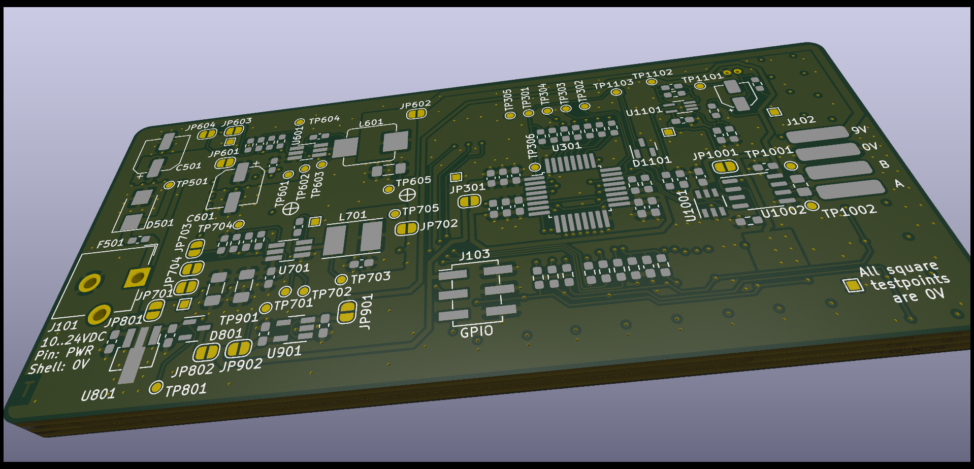
Probing In Circles
If you were to look closely at the test points on the board, you might notice two things:
- There are square pads and there are round pads.
- The round pads are on a circle surrounding the square pads.
You might also have read in the silk screen that the square pads are 0 Volt (also known as Ground).
The idea behind this peculiar test point layout is that all test points can be probed with a ground spring attached to the probe. This eliminates the hassle of trying to connect the probe ground lead. It also eliminates the use of the ground lead as a whole. This in turn makes for much cleaner measurements as ground leads are prone to picking up interference and contribute to ground bounce in the signal.
It took some time to adjust the layout to do this, but I think it’s worth the extra effort as it makes it so much easier to probe the circuit. Of course, not every board may enough space to spare for such a layout. But if it has, I would recommend adopting this layout.
This design, too, is available under the CERN-OHL-S license from my Gitlab repository.
In the next post the controller board will be built and tested.